Sunday, October 30, 2022

Don't copy that IP

Making copies of other people's IP is a terrible thing! And it's a really big problem in the EDA world.


Oh, I'm not talking about the legal aspects. That's something I happily leave to the lawyers. No, I'm talking about making copies of source code instead of referencing the original code. It's a big problem because suddenly you have two different versions, and the chances that a fix that was done in one version will reach the other version are slim to none. When I was entering the world of open source silicon around 2010, this was how things were normally done. And my first reaction was to try and upstream all fixes to IP cores that I found in various projects that were using those cores. My second reaction was to try and find a more sustainable way to avoid this problem in the first place. And solving this problem was one of the initial driving forces behind FuseSoC, and it still is. So it makes me very very sad when, twelve years later, I still find random copies of IP cores, all with various subsets of fixes applied to them.

When we started working on the OpenLANE Edalize backend, one important thing was to have as many example designs as possible, both to make sure the backend was flexible enough to cover all use-cases and also to have a good set of examples for anyone interested in adding FuseSoC support for their own cores. We found a number of example designs in the OpenLANE repository which were used to test OpenLANE itself. Great! ...except... it turned out most of the examples were cores or parts of cores copied from various places. So we did what every sensible person (not really) would do. We decided to upstream all those example designs, so that the OpenLANE support and any other fixes would benefit all users of that IP core.

Bringing' it all back home

At the time we started looking at this, there were 32 different example designs. Our first job was to find out where on earth all these came from. That took a fair amount of detective work, but in the end we found what we believe is the proper upstream for all, except perhaps for one where we are a bit unsure. In that case we chose to file a PR against OpenLANE since that was the closest we could get to an upstream. A few designs were dropped from the OpenLANE examples while we were working on this, in which case we also chose to ignore them.

Once we had identified the origin, we tried to figure out how they worked and then set off to add FuseSoC support for each and every core. At the minimum we added a target for linting and a target for building with OpenLANE through the Edalize backend. In the cases where we found testbenches, we also added support for running those, with a few exceptions where that required tools we didn't have access to.

In addition to adding FuseSoC support, we also added support for running the targets as GitHub CI actions, so that every new commit to the project would automatically lint, build a GDS with OpenLANE and potentially run some testbenches.

And finally we packaged it all up and sent a humongous number of pull requests to different projects with detailed instructions how they could use this. Many of these pull requests have been accepted, but not all. There's not much more we can do about that however. If you are curious, it's possible to check the progress here

So, what does this really mean? Did we make the world a better place for you and for me and the entire human race? I like to think so. At least we didn't make it worse. There are a couple of very real benefits to this work.

  • Adding FuseSoC support makes it eaiser for other users to use these cores in their own projects
  • Adding testbench targets makes it easy for other people to check the cores work as expected
  • Adding a lint target makes it easy to check code quality. Far from all of the designs we encountered pass the lint check
  • On a few occasions, fixes had been made in the copies. These were fed upstream to benefit all users of those cores
  • The CI actions makes it easy to check nothing breaks on future updates of the cores
  • We could test the Edalize OpenLANE backend on a number of different designs to ensure it was flexible enough to handle them all
  • We now have a large pool of example designs for anyone interested in doing the same for their cores
  • And finally, we have seen that some of the maintainers whose cores we added support for, have started doing the same on their other cores, which is fantastic to see.

Now, our hope is of course that you too will be bitten by the FuseSoC fever and add support for your cores too so that we can keep growing the ecosystem of FuseSoC-compatible cores, which in turn will help the EDA tool developers improve their tools.

This work was sponsored by a grant from NLNet Foundation

From simulation to SoC with FuseSoC and Edalize

As you probably also know by now there is a fully open source ASIC toolchain called OpenLANE + a 130nm PDK from SkyWater Foundries together with a program called OpenMPW which allows anyone to produce ASICs from their open source RTL designs completely for free.

And regular readers probably also know that NLNet Foundation has kindly sponsored an Edalize backend for this toolchain, so that users can easily run their designs through this toolchain just as they would do with a simulation environment or an FPGA implementation.

But wouldn't it be great if there also was a good example design to show how this is actually accomplished? And wouldn't it be good if this example design was small enough to quickly run through the tools but still complex enough to showcase several of the features that users might want to use in their own designs.

Well, what better design could exist than a small SoC based on the award-winning SERV, the world's smallest RISC-V CPU? This tutorial will show we can take an existing building block, in this case SERV, turn it into an ASIC-friendly SoC, run it in simulation, make an FPGA prototype and finally have it manufactured as an ASIC. All using FuseSoC and Edalize to hide most of the differences between these vastly different tool environments. Afterwards, you should be able to use the same process and thinking to turn your own designs into FuseSoC packages that can be used with different tools and easily reused in your own and other people's designs.

From design to simulation to FPGA to ASIC. FuseSoC+Edalize helps you all the way


Let's start by looking at what we can do to make an ASIC-friendly SoC out of our good friend SERV.

Creating an ASIC-friendly SoC

For FPGA implementations, there is a reference design for SERV called the Servant SoC. That one is unfortunately not so well suited for ASIC implementation for two reasons. The main one being that it relies on the data/instruction memory being preinitialized with an application that we can run, which is not something we can easily support in an ASIC. The other thing is also memory-related. The Servant SoC uses a separate memory for RF and for instruction+data but SERV supports using a a single shared memory for that, which will allow for an even smaller footprint.

Servant SoC - the reference platform for running SERV on FPGA


So with these things taken into consideration, we look at how to design our SoC called Subservient. An obvious inspiration for this is the Serving SoClet which uses this aformentioned shared memory setup. For the subservient SoC however we need to move the actual RAM macro out of the innards of the design so that we can instead connect the RAM and the subservient SoC as hard macros. Related to this we also introduce a debug interface that we can use to write to the memory while SERV is held in reset since we can't rely on preinitialized memory content.

The Serving SoClet. A building block for making tiny SoCs. Just add peripherals.
 

We can reuse the arbiter and mux from the serving SoClet as is (reuse is good!), but use a slightly modified version of the RAM IF that basically just introduces a Read Enable for the RAM. The debug interface is just a dumb mux that assumes there aren't any memory accesses in flight when the switch is toggled. The RAM interface module that turns the internal 32-bit accesses to 8-bit accesses towards the RAM is the only moderately complex addition, and this is a great thing! It means that we have been able to reuse most of the code and have less untested code to deal with. The resulting architecture looks like this.

The core of the Subservient SoC. Made for portable ASIC implementation. Needs RAM, peripherals and a way to initialize the instruction/data memory
 

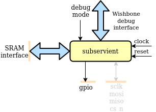
The subservient_core exposes a Wishbone interface where we can hook up peripheral devices. Since we want the simplest thing possible, we just terminate the peripheral bus in a 1-bit GPIO controller and make a wrapper. The greyed out blocks are potential future additions.

The simplest I/O configuration for Subservient. Just a single output pin

 And for someone looking at it from the outside, it looks like this.


Now that we have a design we want to do some testing. For this, we create a testbench that contains a SoC hooked up to a model of the OpenRAM macro that we intend to use in the SkyWater 130nm OpenMPW tapeout and a UART decoder so that we can use our GPIO as a UART. We also add some hastily written lines of code to read a Verilog hex file and write the contents to memory through the debug interface before releasing the SoC reset. This task would be handled by the Caravel harness in the real OpenMPW setup.

Subservient testbench. Starts by loading a program to the simulated RAM through the debug interface and then hand over to SERV to run.


Adding FuseSoC support

We are almost ready to run some simulations with FuseSoC. The last thing remaining is just to write the core description file so that FuseSoC knows how to use the core. Once you have a core description file, you will be able to easily use it with almost any EDA tool as we will soon see. Having a core description file is also an excellent way to make it easier for others to use your core, or conversely, pull in other peoples cores in your design.

We begin with the CAPI2 boilerplate.

CAPI=2:

name : ::subservient:0.1.0


Next up we create filesets for the RTL. Filesets are logical groups of the files that build up your design. You can have a single fileset for your whole design or a fileset each for your files. The most practical way is often to have a fileset for the core RTL, one for each testbench, and separate ones for files that are specific for implementation on a certain FPGA board etc. This is also what we will do here.

Filesets is also where you specify dependencies on other cores. In our case, subservient_core instantiates components from the serving core (or package to use the software equivalent of a core) so we add a dependency on serving here. The serving core in turn depends on the serv core. This means we don't have to care about the internals of either serving or SERV. Their respective core description files take care of the details for us. And if some larger project would want to depend on the subservient SoC, the core description file we are about to write will take care of that complexity for them.

The testbench fileset uses an SRAM model available from a core called sky130_sram_macros and also our trusty testbench utility core, vlog_tb_utils. Finally we add a couple of test programs in Verilog hex format.

filesets:
  core:
    files:
      - rtl/subservient_rf_ram_if.v
      - rtl/subservient_ram.v
      - rtl/subservient_debug_switch.v
      - rtl/subservient_core.v
    file_type : verilogSource
    depend : [serving]

  mem_files:
    files:
      - sw/blinky.hex : {copyto : blinky.hex}
      - sw/hello.hex  : {copyto : hello.hex}
    file_type : user

  tb:
    files:
      - tb/uart_decoder.v
      - tb/subservient_tb.v
    file_type : verilogSource
    depend : [sky130_sram_macros, vlog_tb_utils]

  soc:
    files:
      - rtl/subservient_gpio.v
      - rtl/subservient.v
    file_type : verilogSource


We then define the user-settable parameters to allow us to easily change test program from the command-line, experiment with memory sizes and decide whether the GPIO pin should be treated as a UART or a regular I/O pin.

parameters:
  firmware:
    datatype : file
    description : Preload RAM with a hex file at runtime
    paramtype : plusarg

  memsize:
    datatype    : int
    default     : 1024
    description : Memory size in bytes for RAM (default 1kiB)
    paramtype   : vlogparam

  uart_baudrate:
    datatype : int
    description : Treat gpio output as an UART with the specified baudrate (0 or omitted parameter disables UART decoding)
    paramtype : plusarg


Finally we bind it all together by creating a simulation target. Targets in the core description files are end products or use-cases of the design. In this case, we define a target so that we can run the design within a testbench in a simulator. The targets is also where we reference the filesets and parameters that were defined earlier. This allows us to use different subsets of the core for different targets. We also throw in a derivative sim_hello target as a shortcut to run the other test program, a default target and a lint target so that we can get quick feedback on any potential design mistakes.

targets:
  default:
    filesets : [soc, core]

  lint:
    default_tool : verilator
    filesets : [core, soc]
    tools:
      verilator:
        mode : lint-only
    toplevel : subservient

  sim: &sim
    default_tool: icarus
    filesets : [mem_files, core, soc, tb]
    parameters :
      - firmware
      - memsize
      - uart_baudrate
    toplevel : subservient_tb

  sim_hello:
    <<: *sim
    parameters :
      - firmware=hello.hex
      - memsize=1024
      - uart_baudrate=115200


With this in place we can now run

$ fusesoc run --target=sim_hello subservient

which will run the testbench with the hello.hex program loaded and the GPIO output interpreted as a UART with 115200 baud rate. The output should eventually look something like this.

Running our first FuseSoC target on Subservient

We can run any other program like this, for example the blinky example which toggles the GPIO pin on and off, by supplying the path to a verilog hex file containing a binary

$ fusesoc run --target=sim subservient --firmware=path/to/subservient/sw/blinky.hex

 We won't go into detail on how to prepare a Verilog hex file, but there's a Makefile in the subservient sw directory with some rules for to convert an elf to a hex file.

And as usual, you can list all targets with

$ fusesoc core show subservient

and get help about all available options for a specific target by running

$ fusesoc run --target=<target> subservient --help

Prototyping on FPGA

All right then. Simulations are nice and all, but wouldn't it also be good to have this thing running on a real FPGA as well? Yes, but let's save ourselves a bit of work. In the simulation we could load a file through the debug interface from our testbench. In the ASIC version, that task will be handled by someone else. But to avoid having to implement an external firmware loader in Verilog for the FPGA case, we use the FPGA's capability of initializing the memories during synthesis instead. Remember, always cheat if you have the option!

What board we want to use does not really matter. We can probably just take any random board we have at hand and add the proper pinout and clocking. I happened to have a Nexys A7 within arm's reach so let's go with that one.

We put the FPGA-specific clocking in a separate file so that we can easily switch it out if we want to run on a different board. Next up we add an FPGA-compatible SRAM implementation that supports preloading. We can steal most of the logic for the memory and clocking as well as a constraint file from the Servant SoC (Remember, always steal if you have the option!). Finally we add the subservient SoC itself, connect things together and put them in a new FPGA toplevel like this.

FPGA-friendly version for quick prototyping of our ASIC-friendly SoC

We're now ready to build an FPGA image but it's probably a good idea to run some quick simulations first to check we didn't do anything obviously stupid. All we need for that is a testbench, and since the Subservient FPGA SoC is very similar to the Servant SoC from the outside, we just take the Servant testbench and modify it slightly. We also put in a clock generation module that just forwards the clock and reset signals. With the code in place we add the necessary filesets

  fpga:
    files:
      - rtl/subservient_generic_sram.v : {file_type : verilogSource}
      - rtl/subservient_fpga.v : {file_type : verilogSource}
    
  fpga_tb:
    files:
      - tb/subservient_fpga_clock_gen_sim.v : {file_type : verilogSource}
      - tb/subservient_fpga_tb.cpp : {file_type : cppSource}

and the target for the fpga testbench

  fpga_tb:
    default_tool : verilator
    filesets : [core, soc, mem_files, fpga, fpga_tb]
    parameters: [firmware, uart_baudrate=46080]
    tools:
      verilator:
        verilator_options : [-trace]
    toplevel: subservient_fpga

to the core description file. Note that we're using a baud rate of 46080. That's because we define the testbench to run at 40MHz instead of 100MHz (for reasons that will become clear later) and then we must scale down that baud rate to 40% of 115200. Let's give it a shot by running

$ fusesoc run --target=fpga_tb subservient

Works in simulation! This increases our confidence in the FPGA implementation

Works like a charm. Now we have more confidence when going to FPGA.

There are a couple of things that differ between our simulation and an actual FPGA target. Instead of a testbench we need to add an FPGA-specific clocking module and a pin constraint file for our board. So let's put them in a new fileset and then create a target referencing these files and telling the EDA tool (Vivado) what FPGA we're targeting.


filesets:
  ...
  nexys_a7:
    files:
      - data/nexys_a7.xdc : {file_type : xdc}
      - rtl/subservient_nexys_a7_clock_gen.v : {file_type : verilogSource}

targets:
  ...
  nexys_a7:
    default_tool: vivado
    filesets : [core, soc, mem_files, fpga, nexys_a7]
    parameters: [memfile]
    tools:
      vivado: {part : xc7a100tcsg324-1}
    toplevel: subservient_fpga

 Voilà! Now we can run our FPGA build with

$ fusesoc run --target=nexys_a7 subservient

If everything goes according to plan and we have the board connected, it will be automatically programmed. Using our favorite terminal emulator and setting the correct baud rate should then give us the following output.

Wow! It's just like in the simulation...which is kind of the idea

Alright then, simulation and FPGA is all good, but our original idea was to put this in an ASIC. Sooo....how do we do that?

Making an ASIC target

The good news is that we have actually done most of the work already, and this is very much the point of FuseSoC and Edalize. It allows you to quickly retarget your designs for different tools and technologies without having to do a lot of tool-specific setup every time. Now, OpenLANE is a bit special compared to other EDA tool flows so there will be a couple of extra bumps in the road, but hopefully these will be smoothed out over time.

Since we have an Edalize backend for the OpenLANE toolchain already, all we need to to is to add any technology- and tool-specific files and invoke the right backend. OpenLANE can be operated in several different ways, but the way that Edalize integration currently works is by adding TCL files with OpenLANE configuration parameters that will be picked up by OpenLANE and then Edalize assumes it will find an executable called flow.tcl and that a usable PDK is installed and can be found by OpenLANE.

So on the tool configuration side, all we need to do is to add a TCL file containing the parameters we want to set. And the only things we are strictly required to put into this file is information about the default clock signal and target frequency.

set ::env(CLOCK_PERIOD) "25"
set ::env(CLOCK_PORT) "i_clk"

There are a million other parameters that can be set as well to control size, density and different routing strategies so I encourage everyone to read the OpenLANE docs and experiment a bit, but for this time we just add the aforementioned settings to a tcl file and add a fileset and target.

filesets:
  ...
  openlane:
    files:
      - data/sky130.tcl : {file_type : tclSource}

targets:
  ...
  sky130:
    default_tool: openlane
    filesets : [core, soc, openlane]
    parameters :
      - memsize
    toplevel : subservient

Seriously, it's not harder than that. We're now ready to run OpenLANE and have our GDS file. The thing is, though, that it can be a bit finicky to install the toolchain and the PDK. Building the PDK from sources using the official instructions requires downloading gigabytes of Conda packages, keeping track of a number of git repositories and an somewhat convoluted build process. There are several disjointed attempts at providing a pre-built PDK but at the time of writing there didn't seem to be an agreement on how to do that. Also, the OpenLANE toolchain itself is a bit special in that the recommended way of running it is from a Docker image rather than install it directly. So, with these two facts at hand we decided to simply prepackage a Docker image with OpenLANE and a PDK included. This image gets updated from time to time, but in general it's a bit behind the upstream version. But that's totally fine. There's seldom any need for running the absolutely latest versions of everything.

Launcher scripts

But how then do we run OpenLANE from the Docker image? For that we use another one of Edalize's nifty features, launcher scripts! Normally, Edalize calls the EDA tools it wants to run directly but we can also tell Edalize to use a launcher script. A launcher scripts is a script (or any kind of program, really) that gets called instead of the EDA tools. The launcher script is also passed the original command-line as parameters so that it can make decisions based upon what Edalize intended to originally run.

In this case, Edalize wants to run flow.tcl -tag subservient -save -save_path . -design . when we invoke the OpenLANE backend but telling Edalize to use a custom launcher that we choose to call el_docker, the command-line instead becomes el_docker flow.tcl -tag subservient -save -save_path . -design .

If we just want the launcher script to do something special when OpenLANE is launched, then we simply check if the first argument is flow.tcl. In that case we do something special, or otherwise call the original command-line as usual. Simple as that.

So what special magic do we want to do for OpenLANE? We want to run flow.tcl from our OpenLANE+PDK Docker image and at the same time make our source and build tree available within the image. The whole command in its simplest forms looks something like this when invoked from the Edalize work root

$ docker run -v $(pwd)/..:/src -w /src/$(basename $(pwd)) edalize/openlane-sky130:v0.12 flow.tcl -tag subservient -save -save_path . -design .

We could make this script a bit nicer if we want so that we run as the ordinary user instead of as root, and so on, but this has in fact already been taken care of. The aforementioned el_docker launcher script already exists and is installed together with Edalize. And not only does it support running OpenLANE through Docker but also a whole bunch of other tools like verilator, icarus, yosys, nextpnr and so on. So you can just as well use this script for simulation and FPGA purposes if you for some reason don't want to natively install all these EDA tools. The proprietary tools are for obvious reasons not runnable this way since the EDA vendors would probably get very, very angry if we put their precious tools in containers and published them for everyone to be used. Hopefully we can completely avoid proprietary tools some day, but not yet. Anyway, so how do we tell Edalize to use a launcher script? Currently, this is done by setting the EDALIZE_LAUNCHER environment variable before launching FuseSoC (which launches Edalize).

So, our final command will be:

$ EDALIZE_LAUNCHER=el_docker fusesoc run --target=sky130 subservient

And with that, my friends, we have built a GDS file for the Subservient SoC that we can send to the fab and get real chips back. And this we did, but that's for another day. So let's just lean back and take in the beauty of the world's smallest RISC-V SoC, created by open source tools, and think a bit about how incredibly easy it was thanks to FuseSoC and Edalize (and of course NLNet who funded the Subservient SoC and integration of OpenLANE and Edalize).

 And now, it's your turn to do the same with your own designs. Good luck!


Friday, October 14, 2022

SERV: The Little CPU That Could

Big things sometimes come in small packages. Version 1.2.0 of the award-winning SERV, the world's smallest RISC-V CPU has been released and it's filled to the brim with new features.

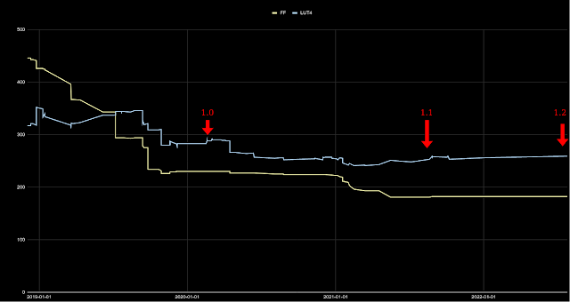
Historically, focus has always been on size reduction, making it ever smaller, and that has paid off. It's now about half the size of when it was first introduced. But at this point we're not really getting much smaller, and frankly, that's fine. It still is the world's smallest RISC-V CPU by a good margin.


Resource usage over time for the SERV default configuration


Mimimum SERV resource usage for some popular FPGA families


So this time we focus on features instead. Most notably we have support for two major ISA extensions, both often requested by users, but there are also a number of other new features as well. Let's take a look at all of them, shall we?

M extension


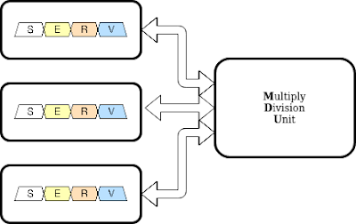
Multiple SERV cores can share one MDU (or perhaps other accelerators)

As part of Google Summer of Code 2021, Zeeshan Rafique implemented support for the M ISA extension. This was done through an extension interface that allows the MDU (Multiplication and Division Unit) to reside outside of the core and potentially be shared by several SERV cores in the same SoC, or integrated into other RISC-V cores for maximum reusability. We hope to also see other accelerators use the extension interface soon. Zeeshan's report about the project to add the M extension can be read here

C extension

Two extra blocks to save a lot of memory


As part of the Linux Foundation Mentorship program Spring 2022, Abdul Wadood has implemented support for the C ISA extension. The C extension has been the most requested feature of SERV. Since SERV is so small, the memory typically dominates the area and the C extension has the potential to allow for smaller memories and by extension a smaller system. Abdul's report about the project to add the C extension can be read here

Documentation

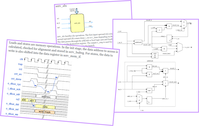
Pictures and words. The SERV documentation has it all
 

Documentation continue to improve with more gate-level schematics, written documentation, source code comments and timing diagrams towards the goal of becoming the best documented RISC-V CPU. There are always room for improvements, but now all modules as well as the external interfaces are at least documented.

Bug fixes

A bug that caused immediates to occasionally get the wrong sign (depending on which instruction was executed prior to the failing one) was found and fixed.
Model/QuestaSim compatibility has been restored after accidentally being broken after the 1.1.0 release and a few more resets have been added after doing extensive x-propagation analyses.
 

Compliance tests

Version 2.7.4 of the RISC-V compliance test suite is now supported over the older 1.0 release. A Github CI action has also been created to test the compliance test suites with all valid combinations of ISA extensions for improved test coverage.

Servant

Moving outside of the SERV core itself we have Servant, the simple SERV reference SoC. Servant isn't the most feature rich SoC, instead focusing on simplicity, but it has at least the bare minimum to run the popular Zephyr Real Time Operating System. During this development cycle Servant, has gained support for five new FPGA boards: (EBAZ4205, Chameleion96, Nexys2 500, Nexys2 1200 and Alinx AX309)
With this, the total number of officially supported boards is 26.

ViDBo support


Got no FPGA board? Don't worry. ViDBo has you covered.


Support for the Virtual Development Board protocol has been added, making it possible to interact with a simulation of an FPGA board running a SERV SoC, just as it would be a real board. This allows anyone to build software for SERV and try it in simulation without access to a real board.

OpenLANE support

A few thousand transistors needed to build the world's smallest RISC-V CPU


Thanks to the FOSSi OpenLANE toolchain, SERV can be implemented as an ASIC with the SkyWater 130nm library. It has also been taped out as part of the Subservient SoC but at the time of this release the chips have not yet returned from the fab. Thanks to the combination of a FuseSoC, a FOSSi ASIC toolchain and publicly available CI resources however, a GDS file of SERV is now created on every commit to the repository, making the ASIC process about as agile as it can get.

The future

So what lie as ahead for our favorite CPU? Well, there were a number of features that I decided to postpone in order to get a new version released. There were plenty of big features anyway

DSRV & QERV

Smaller or faster. The choice is yours.


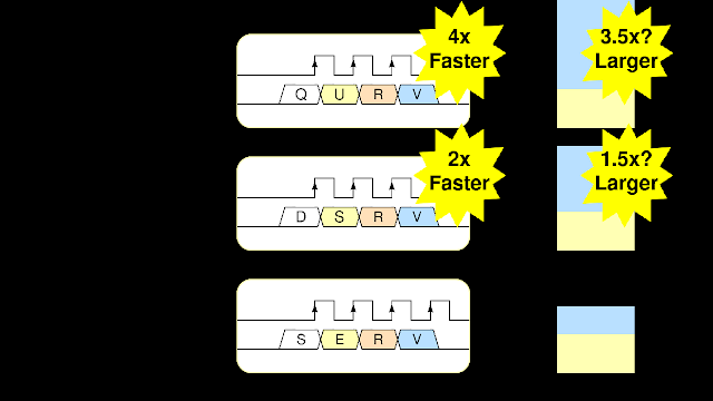
SERV is very small. That's kind of the point. However, many times it's preferable to use slightly more resources if it also means faster. Changing to a 2-bit datapath would make SERV twice as fast, while likely using far less than twice as much logic. Moving to a 4-bit datapath would halve the CPI once again. The 2- and 4-bit versions are tentatively called DSRV, for Double SERV, and QERV, for Quad SERV. I think you get the point, but here's a video explaining the idea in slightly more detail if anyone is interested in taking up this as a project.

While we could theoretically go for 8-, 16- and 32-bit versions as well, there are some internal design choices that would make this more complicated and it would probably be a better idea to design a new implementation from scratch for 8+ bit datapaths.

Decoder generator

Another big thing that I had hoped to finish but decided to push to a future version is autogenerated decoder modules. I have spent a lot of work on it and I think it's a really interesting idea that might even end up as a paper at some point. Unfortunately I don't have the time to finish it up right now. So, what's it all about? Well, it's a bit complicated so I think it's best to leave the details to a separate article (which I hope to find time to write soon), but the overall idea is to take advantage of the fact that many internal control signals are irrelevant when executing some class of instructions, so that we can combine them with other control signals that are irrelevant for other classes of instructions.

Servant

I was also hoping to add some improvements to Servant, the SERV reference platform but couldn't find time for that either. I think that's ok though. Anyone who's looking for a more advanced platform to run SERV should go for Litex instead which supports SERV already. Fellow RISC-V ambassador Bruno Levy even demonstrated that it was possible to run DooM on SERV through Litex, I might be a bit partial, but it's a beautiful thing to see this tiny thing take on such a big task and as a proud parent I look at it and wonder is there anything this little CPU can't do with a little encouragement.

Saturday, October 1, 2022

It's time to to thank UVM and say goodbye

UVM has been a massive success. There's no doubt about that. For the first time it showed the chip industry the benefits of having a common framework. You can hire directly for UVM skills. Vendors provide UVM models for interfacing their IP. There are tools for generating UVM registers and other boilerplate code. There is training available and forums for asking UVM-related questions.

But it wasn't always like that. I remember when UVM was still not widely adopted. A lot of companies said "Weeeell, I'm sure this UVM thing is very good for other companies, but you know, our needs are a bit special". It's funny how all those special needs just suddenly disappeared when the economic benefits of not having to deal with your own framework and being able to easily hire people and get VIP from vendors became apparent.

So UVM has been a massive success. It has become so ubiquitous so that many people in the industry seem to believe it has some magical properties and that it's the only way to verify chips. But, frankly speaking, it's not really that good of a framework. It's clunky and suffer from a lot of legacy. Many companies I'm talking with don't actually use it as is but have written some custom framework on top, and you can find plenty of tools to  generate UVM, which in the end means we end up with a boatload of incompatible framework generators instead. But the biggest issue is that it's written in SystemVerilog.


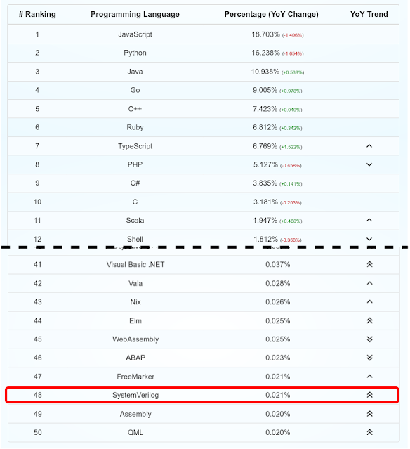
Oh no! Will this turn in to one of those language wars again? Maybe, but we can't ignore the fact that there probably goes 1000 Javascript, Python or Java developers for each Verilog coder. (System)Verilog (or VHDL for that matter) barely scrapes the bottom of the top 50 most popular language lists.  "Nonsense!", I hear my fellow chip design engineers mumble, "Everyone knows Verilog". Well, there's a word for that. Survivor bias. Everyone in the semiconductor industry knows Verilog because those who couldn't stand the language just went elsewhere. And this is a huge problem for the industry. On top of an aging demographic we have issues keeping the youngsters interested when there's other fancier languanges and environments out there.


Github Language Stats (https://madnight.github.io/githut)

"But! But!...", you argue, "...you need Verilog to work with chip design". I won't argue that in practice this is true to some degree because there's a whole lot of verilog out there, but in theory Verilog doesn't say absolutely anything about how chips work. It's just a programming language, which original intended purpose was to describe chip behavior. Remember, Verilog wasn't ever meant to be used to implement chips, which is a fact that tends to get forgotten many times. As another example of this, look at Erlang, which was created to program telephone switches. This means neither that Erlang can't be used for other things, nor that Erlang is the only way to program telephone switches.

"Still.. ", I hear from the back of the room, "..can't they just learn SystemVerilog? It's like C++, sort of". That misses a large part of what makes a language successful. True, it's a C-like syntax to some extent (mixed up with Java and a hodge-podge of 90's language ideas), but you don't have access to your toolbox of C++ tools like linters, debugger, syntax highlighters, IDEs, sanitizers and everything else that makes you productive. While the chip designers might think SystemVerilog is the best option because it has the largest ecosystem in this domain, this ecosystem is a drop in the ocean compared to popular languages.

And I'm 100% certain that in many cases, although it's beneficial, you don't need to know a single thing about how chips work and you can still do a great job of verifying the functionality of some IP core. Let's turn things around for a while. I have spent the past ten years developing military radar, software defined radios, automotive radar, digital cameras, weather radar to name a few things. And I have absolutely no clue about how microwaves work and I'm a lousy photographer, but I still can do a good job because at the abstraction where I work I don't need to understand all these things. But if I also would be required to learn, let's say Fortran, because that's what was traditionally used for math heavy applications. well, then I would probably start looking for jobs elsewhere. And the same goes for verification engineers. Give them a spec, tell them what to do and a familiar programming languages and they'll probably do just fine. I definitely think it's preferable to have someone who does know how chips work on the team, but it doesn't have to be all of them.

So let's assume then that we can have verification engineers who don't have to know verilog. What does that mean? Well, it means that our pool of potential candidates has grown by a 1000 times. I can tell you for sure that it will be a lot easier to find good verification engineers than finding good vericication engineers who also happen to know Verilog. And if you have ever experienced how hard it is to get good verification engineers, then this is something you will greatly appreciate. And it's not just the number of developers that's growing. The whole flourishing ecosystem of libraries, forums and examples around popular languages like Python makes the Verilog ecosystem look like a wasteland and this means you can reuse much more existing code and involve your software friends in better ways.

So what's the solution then? We need to enable software developers to create and verify chips. In this article we will be looking at the verification side, but I suggest looking at companies like ChipFlow to see what's happening on the design side as well. And Python is a good bet right now. It might be Go or Rust or something completely different in a couple of years, but right now Python is widely used already as a glue language in chip development environments, like perl was used 10-20 years ago. And we see more and more EDA tools growing Python bindings. I'm not sure the latter is a purely positive thing, but we'll see.

And when it comes to Python and verification I have said many times by now that I believe cocotb will be one of the important technologies in the coming years. It is a mature technology that is already adopted by large and small companies and you can find ads for companies looking to hire for this skill. And just like we saw with UVM, being able to hire for a certain skill without having to train them for your home-built verification framework is a time and money saver. Another thing that speaks for cocotb is that it uses your regular RTL simulators. This means it poses no threat to the EDA vendors. It just enhances their offering and they can continue to sell licenses for their tools. And with cocotb being a project governed by FOSSi Foundation, we clearly see how much more interested the EDA vendors are in collaborating on cocotb compared to many other free and open source silicon projects. Of course, it also works with your favorite open source simulators like Icarus, ghdl or Verilator and this means the proprietary EDA vendors need to compete with the open source tooling on equal terms, where they need to flex the strengths of their tooling rather than the artificial lock-in created because none of the open source tools have any UVM support to speak of.

So, to sum things up. UVM has been a massive success and has seen industry-wide adoption over the past ten years. But the most important thing UVM did was probably to show the industry the benefit of having a common framework, not being the best framework in itself. My prediction is that UVM will see a slow (everything in EDA is slow) decline in the coming years and it will be relevant for long time, but gradually be replaced by frameworks written in more common languages and that it's a good bet to get to know cocotb specifically a little better. So I think it's time to consider whether UVM sparks joy. Otherwise, it's time to thank it and say good bye.


Now, if the industry could just agree on a common format for describing IP cores and interfacing EDA tools. Oh well. That's another battle for another day.